Silicon carbide processing technology
Silicon carbide wafers use high-purity silicon powder and high-purity carbon powder as raw materials, and use physical vapor transmission (PVT company) to grow silicon carbide crystals and process them into silicon carbide wafers.
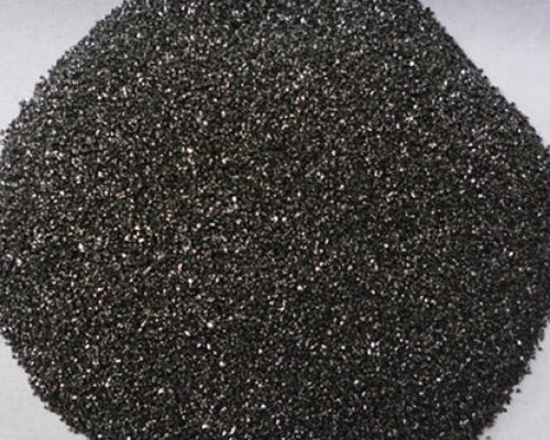
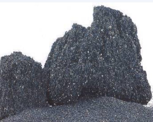
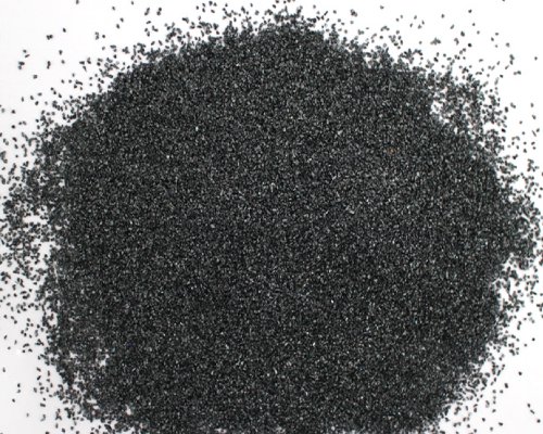
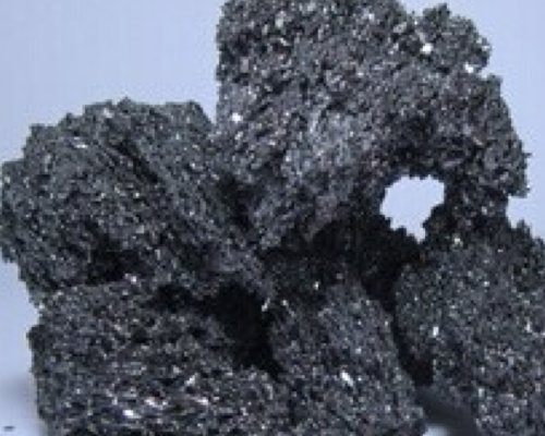
(1) Raw material synthesis. Mix high-purity silicon powder and high-purity carbon powder in a certain proportion, and the silicon carbide particles are reacted and synthesized at a high temperature of 2,000 °C. After crushing, cleaning and other processes, high-purity silicon carbide particles that meet the requirements of crystal growth are obtained. Silicon carbide micro powder raw material.
(2) Crystal growth. Using high-purity silicon carbide powder as raw material, using an independently developed crystal growth furnace, silicon carbide crystals are grown using the physical vapor transport method (PVT method).
Place high-purity silicon carbide powder and seed crystals at the bottom and top of a cylindrical sealed graphite crucible in a single crystal growth furnace, respectively.
The crucible is heated to above 2000°C through electromagnetic induction, and the temperature at the seed crystal is controlled to be slightly lower than the temperature at the bottom of the micropowder, forming an axial temperature gradient in the crucible.
Silicon carbide powder sublimates at high temperatures to form Si2C, silicon carbide, Si and other substances in the gas phase, and is driven by the temperature gradient to reach the seed crystal at a lower temperature, and crystallizes on it to form a cylindrical silicon carbide ingot.
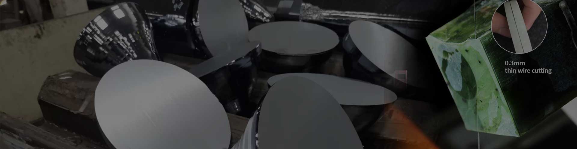
(3) Ingot processing. The prepared silicon carbide ingot is oriented using an X-ray single crystal orientator, and then grounded, rolled out, and cut into silicon carbide standard diameter size crystals. The latest process for cutting silicon carbide crystals uses a diamond wire ring saw for Crop.
(4) Crystal cutting. Using multi-wire cutting equipment, silicon carbide crystals are cut into thin slices up to 1mm thick.
(5) Wafer grinding. The wafer is ground to the required flatness and roughness through diamond slurries of different particle sizes.
(6) Wafer polishing. Silicon carbide polished wafers with no surface damage are obtained through mechanical polishing and chemical mechanical polishing.
(7) Wafer inspection.
Use optical microscope, X-ray diffractometer, atomic force microscope, non-contact resistivity tester, surface flatness tester, surface defect comprehensive tester and other equipment to detect microtube density, crystal quality, surface roughness, resistivity, warpage Curvature, curvature, thickness variation, surface scratches and other parameters of silicon carbide wafers, and determine the quality level of the wafers accordingly.
(8) Wafer cleaning. The silicon carbide polished wafer is cleaned with cleaning agent and pure water to remove residual polishing fluid and other surface contaminants on the polished wafer, and then the wafer is blown and dried with ultra-high purity nitrogen and a dryer; clean room packaging In the clean wafer cassette, silicon carbide wafers are formed ready for downstream use.
The larger the wafer size, the more difficult it is to grow and process the corresponding crystals, the higher the manufacturing efficiency of downstream devices, and the lower the unit cost. Now, international silicon carbide wafer manufacturers mainly provide 4-inch to 6-inch silicon carbide wafers, while CREE and International leading companies such as II-VI have also begun investing in the construction of 8-inch silicon carbide wafer production lines.