How to process silicon carbide?
Silicon carbide (sic) materials are the main development direction of the power semiconductor industry. Used in the manufacture of power devices, it can significantly improve power utilization. In the foreseeable future, new energy vehicles will be the main application scenario of silicon carbide power devices.
As a technology pioneer, Tesla took the lead in integrating all-silicon carbide modules3 into Models, and other first-tier car companies are also planning to expand the application of silicon carbide. As the manufacturing cost of silicon carbide devices decreases and process technology gradually matures, silicon carbide The power device industry has broad prospects.
What is silicon carbide?
Silicon carbide (sic) is the third generation compound semiconductor material. The cornerstone of the semiconductor industry is chips. The core materials for manufacturing chips are divided into:
First-generation semiconductor materials (mostly high-purity silicon is currently widely used), second-generation compound semiconductor materials (gallium arsenide, indium phosphide), and third-generation compound semiconductor materials (silicon carbide, gallium nitride).
Due to its superior physical properties: high band gap (corresponding to high breakdown electric field and high power density), high electrical conductivity, and high thermal conductivity, silicon carbide will be the most widely used basic material for manufacturing semiconductor chips in the future.
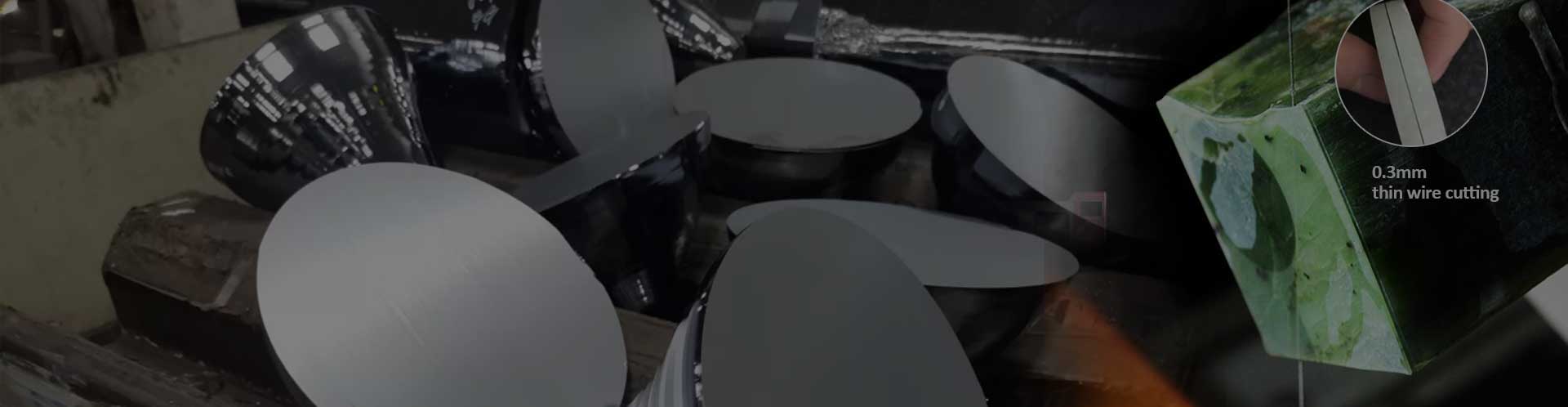
The main form of silicon carbide in semiconductor chips is the substrate. Semiconductor chips are divided into integrated circuits and discrete devices, but whether they are integrated circuits or discrete devices, their basic structures can be divided into “substrate-epitaxial-device” structures. Silicon carbide in The main form in semiconductors is as substrate material.
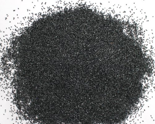
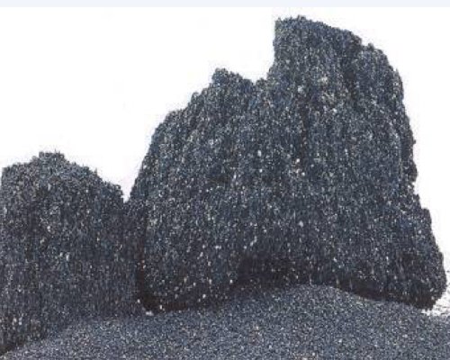
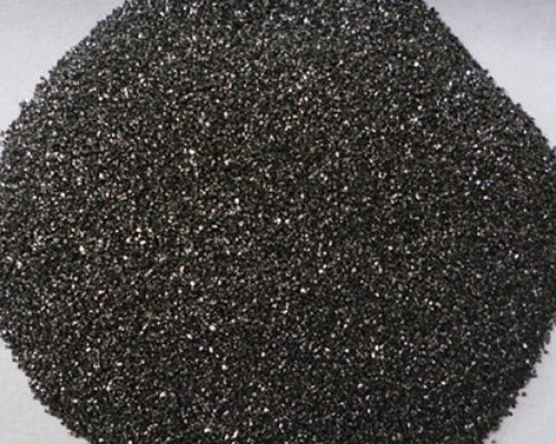
Silicon carbide wafers are single crystal flakes formed through cutting, grinding, polishing, cleaning of silicon carbide crystals and other processes. As a semiconductor substrate material, silicon carbide wafers can be made into silicon carbide-based power devices and microwave radio frequency devices through epitaxial growth. Device manufacturing and other links are important basic materials for the development of the third-generation semiconductor industry.
According to different resistivities, silicon carbide wafers can be divided into conductive and semi-insulating types. Among them, conductive silicon carbide wafers are mainly used to manufacture high-temperature and high-voltage power devices, with a large market size; semi-insulating silicon carbide substrates are mainly used in microwave radio frequency devices and other fields.
With the accelerated construction of 5G communication networks, market demand has increased significantly. The hardness of silicon carbide is second only to diamond. It not only has the characteristics of high hardness, but also has high brittleness and low fracture toughness.