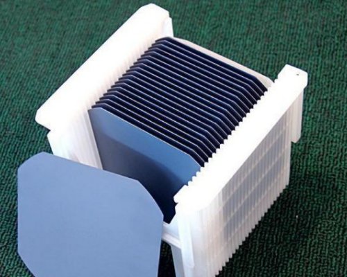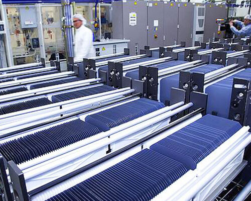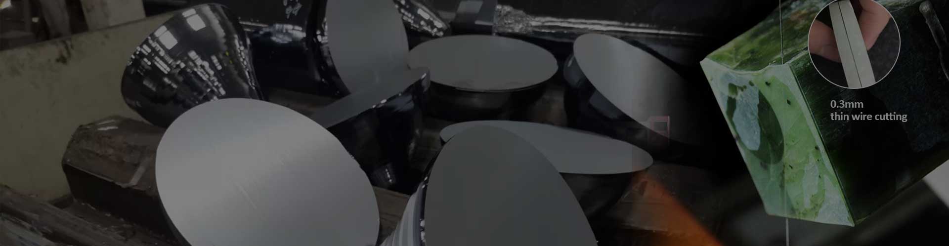
Size changes of photovoltaic silicon wafers
The size of photovoltaic silicon wafers is derived from semiconductor silicon wafers. In terms of development, photovoltaics lag behind semiconductors by 1 to 2 generations. Over the years, the size of semiconductor silicon wafers has continued to increase, and photovoltaic silicon wafers have also experienced a process from small to large.
Driven by cost dilution and component quality improvement, in the 40 years since 1981, the size of photovoltaic silicon wafers has grown from 100mm to 210mm, and the specifications have doubled.
1981-2012: 100mm-156mm
Between 1981 and 2012, the margins of silicon wafers were 100mm and 125mm, and 125mm silicon wafers were dominant. Then, the margins of silicon wafers increased significantly from 125mm to 156mm (ie M0), an increase of 54.1%. 156MM silicon wafers have gradually become a popular choice for P-type monocrystalline silicon wafers and multicrystalline silicon wafers. Around 2014, 125mm P-type silicon wafers are basically eliminated and are only used in some IBC and HIT battery modules.
2012-2018: M0-M2 type
At the end of 2013, LONGi, Zhonghuan, Jinglong, Yangguang Energy, and Comtec took the lead in unifying the M1 (margin 156.75mm, diameter 205mm) and M2 (margin 156.75mm, diameter 210mm) standards to 156.75mm. silicon wafers, which is a major change in the history of silicon wafer size development. In 2017, the size standard was reviewed and approved by the SEMI Standards Committee. The revised version of the national standard for multicrystalline silicon wafers in 2018 also determined 156.75mm as the standard side length, and suggested that future size increases should be changed in multiples of 1 mm.
M2 silicon wafers quickly occupied the market. Until 2018, all mainstream monocrystalline silicon wafers in the industry adopted the M2 standard, with a market share of up to 85%.
According to statistics, M0 and M1 silicon wafers are no longer produced in 2017. In 2019, 156.75mm size market accounted for about 61%. CPIA predicts that the proportion of 156.75mm products will drop significantly in 2020. In 2022, the market will completely bid farewell to 156.75mm size silicon wafers. Block.
2018 to now: M2-M6 type
After the melee, two mainstream sizes appeared in the market: G1 square monocrystalline (158.75mm margin) and M6 (166mm margin) large silicon wafers. In 2018, Jinko took the lead in launching G1 silicon wafers, but when G1 silicon wafers had not yet gained a foothold and the market share was only 10%, Longi launched M6 silicon wafers in June 2019, and at this time Jinko continued to follow up. Starting at 163mm. During this period, Hanwha launched M4 (margin 161.7mm) product source 2019, using 5.7% area increase compared to M2, a small amount exists in the market. The products are mainly N-type bifacial components.
4, Ultimate silicon wafer size: 210mm
In August 2019, Zhonghuan launched G12 (margin 210mm) large silicon wafer, which greatly increased the area of M6 silicon wafer by 60.8%, pushing the silicon wafer size to the extreme, and achieving three negations: negation of existing products, negation of existing technology, and negation of existing self. According to data from Zhonghuan Co., Ltd. , the cost of G12 battery is 25.56% lower than M2, and the component cost is reduced by 16.8%. Compared with 166mm, BOS cost is reduced by 12% in power station construction, and the corresponding levelized cost of electricity is reduced by 4.1%.
However, the discussion about 166 and 210 has never stopped in the industry. The biggest “tangled point” is the advent of production line transformation with 210 silicon wafers. Enterprises need to consider 210 to achieve efficiency improvement, after paying the transformation cost. At the same time, the emergence of new cutting technology has also caused the market to debate whether to use endless diamond wire cutting to replace the traditional diamond wire for silicon ingot cutting process. But it needs to be known that with the large-scale trend of silicon wafers, the transformation of production lines is only a matter of time.