Traditional solar cell production process
In the past, we always described the manufacturing principles and silicon wafer processing technology. Today we will introduce the production technology of traditional solar cells.
Traditional battery production can be mainly summarized into 6 steps. From the perspective of traditional battery manufacturing process, it can be summarized into the following six steps:
1) Cleaning and texturing, the main purpose is to remove various pollutants adsorbed on the surface of the silicon wafer, and remove the cutting damage layer on the surface of the silicon wafer;
The light trapping principle is used to reduce the reflectivity of the battery surface. An uneven surface will increase secondary reflection, change the light path and incident method, increase the absorption of light, increase the short-circuit current, and thereby improve the conversion efficiency of the battery.
Among them, due to the different crystal structures of monocrystalline silicon cells and polycrystalline silicon cells, taking into account efficiency factors, polycrystalline silicon cells are made of acid, and the textured surface is an irregular concave and convex surface;
Monocrystalline silicon cells are made of an alkaline structure, and the textured surface is a regular pyramid structure;
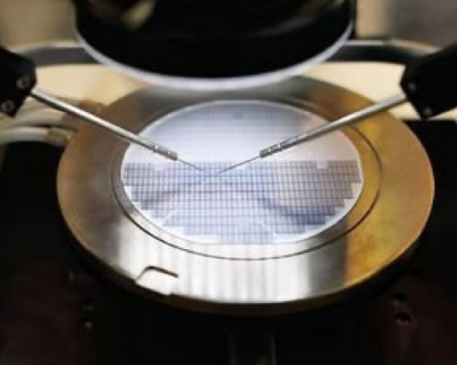
2) Diffusion, the main purpose is to form PN junction, which is the core of battery manufacturing and allows cells to function.
P-type silicon wafers require phosphorus diffusion. Liquid phosphorus source phosphorus oxychloride is the mainstream choice for phosphorus diffusion.
The main reason is that liquid phosphorus source diffusion has the advantages of high production efficiency, good stability, uniform and smooth PN junction, and good diffusion layer surface;
N-type silicon wafers require boron diffusion. Now, the liquid sources for boron diffusion mainly include trimethyl borate, tripropyl borate and boron tribromide. Boron expansion is more difficult than phosphorus expansion.
The main reason is that the solid solubility of boron in silicon is low, and the actual boron diffusion temperature needs to reach 900~1100 degrees Celsius;
3) Etching (dephosphorized silicon glass), during the diffusion process, the side and trailing edges of the silicon wafer are not blocked, and phosphorus will also diffuse.
The photogenerated electrons collected on the front side of the PN junction flow to the back side of the PN junction along the area where phosphorus diffuses along the edge, causing short circuit and battery failure.
The etching process is to remove the phosphorus part on the edge of the silicon wafer to avoid short circuit of the PN junction and reduce the parallel resistance;
4) Clothes, mainly play
a) Anti-reflective effect, improves cells’ absorption of sunlight, increases photogenerated current, thereby improving conversion efficiency;
b) Passivation. The passivation of the battery surface by hydrogen in the film reduces the surface recombination rate of the emitter junction and increases the open circuit voltage, thus improving the conversion efficiency. Common coating technologies in photovoltaic cells include PECVD, liquefied silicone sheet, and PVD Coatings, atomic layer deposition (ALD, etc.;
5) Screen printing, the main function is to collect the current of solar cells and manufacture electrodes, including the first silver electrode on the back, the second, back field printing and drying of the aluminum material on the back, and the printing of the third silver electrode;
6) Sintering, that is, sintering the electrodes printed on the battery surface at high temperature so that the electrodes form ohmic contact with the silicon wafer itself, increasing the open circuit voltage and filling factor of the battery, and making the electrode contacts have resistive characteristics to achieve high conversion efficiency.
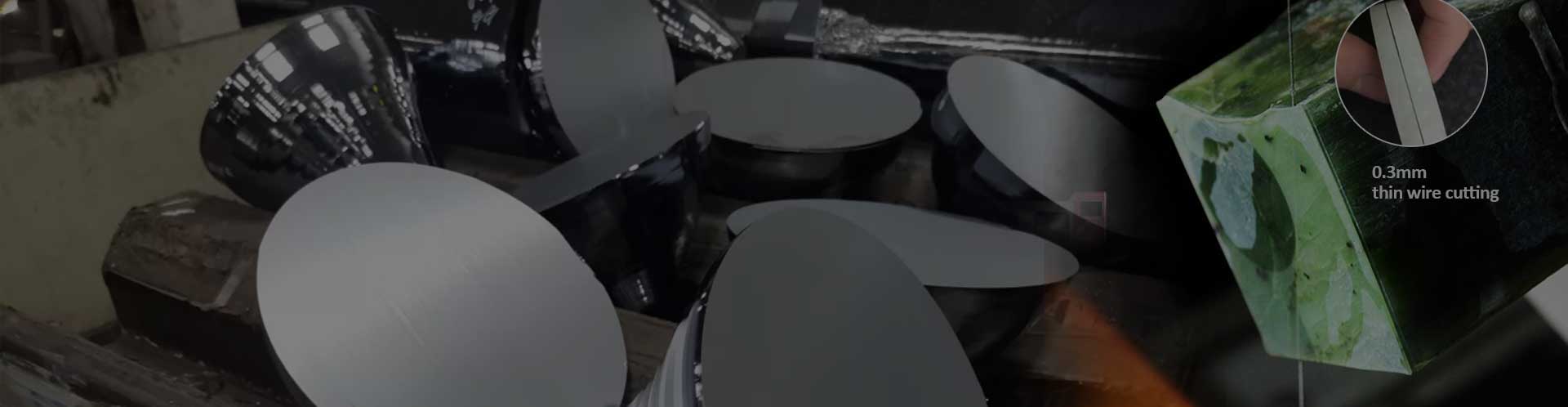
It is not difficult to see from the cell production process that in the early stages of silicon wafer production, the better the cutting surface, the easier it will be to process cells later. Silicon wafer processing technology must not only improve the cutting surface from the cutting of silicon wafers, but also pay attention to the cutting of silicon ingots surface, and gradually improve to obtain a better silicon surface.